
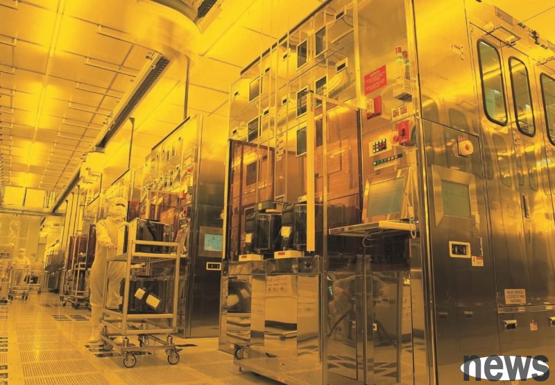
The three major Japanese semiconductor giants have set off a fierce competition for production capacity around the world, which is a prediction of the competition for the next generation of chip manufacturing processes. Tokyo Ohka Kogyo (TOK), JSR Corporation and ADEKA, a Japanese photoresist manufacturer, recently announced multi-billion yen investment plans, representing another profound reshaping of the global semiconductor supply chain. In addition to fighting against South Korea's Samsung and SK Hynix, investment is also preparing for the demand for advanced processes that will explode from 2025 to 2030.
Japan has an overwhelming monopoly in the photoresist field. According to market data, Japanese companies account for more than 91% of the global photoresist market share. Tokyo Chemical Industry alone controls 25.1% of the global market, and high-end EUV photoresists control 45.9% of the market. Tokyo Chemical Industry invested 20 billion yen in South Korea to build a photoresist plant, which will be put into operation in 2030, and will invest an additional 12 billion yen in a high-purity chemical plant. The essence of dual-track investment is to move the supply chain to the geographical location closest to major customers: the home bases of large chip manufacturers such as Samsung and SK Hynix.
According to research by U.S. Bank Group (UBS), Japanese photoresist companies will maintain their advantage at least until 2030. Companies that master the photoresist supply chain within five years will hold the throat of the global semiconductor industry.
JSR Company’s timetable is more aggressive: South Korea’s MOR photoresist factory will begin mass production at the end of next year, two or three years ahead of Tokyo Chemical Industry. Adeka, a century-old company, adopts a "local first" strategy and invested 3.2 billion yen in Japan to build a MOR photoresist factory, with the goal of mass production in April 2028.
The inevitability of South Korea becoming an industrial hubThere are multiple reasons why South Korea has become the first choice for Japanese materials giants to expand production. The South Korean government announced a large semiconductor cluster plan in 2024, with an investment of US$47.1 billion by 2047. The Pyeongtaek-Yongin area in Gyeonggi Province will become the world's largest chip manufacturing center, with a target monthly production capacity of 7.7 million wafers. This area has gathered the world's top chip companies such as Samsung and SK Hynix, and the demand for photoresists and other products has exploded.
SK Hynix will increase its capital expenditure by 75% this year to cope with the crazy demand for high-bandwidth memory (HBM) for artificial intelligence chips. The demand for HBM will increase by 200% in 2024 and will increase by 70% this year. This surge in demand translates directly into an urgent need for higher-order photoresists. At the same time, from a geopolitical perspective, Japanese materials companies building factories in South Korea can also help avoid the risk of trade friction, and localized production can reduce the vulnerability of the supply chain.
According to data from the U.S. International Trade Commission, the global competitiveness of South Korea’s semiconductor industry continues to increase. Samsung's foundry investment in 2nm has been launched, and SK Hynix's capacity expansion plans for advanced processes such as DRAM 1b and 1c have been confirmed. These companies urgently need localized material supply partners to cope with the bottlenecks that global photoresists may face. Japanese companies investing in South Korea are not just building factories, but also forming long-term strategic ties to ensure that when 2-nanometer wafers are industrialized, material shortages will not become a bottleneck in production capacity.
The strategic value of MOR photoresistMOR (metal oxide photoresist) has become the core choice for EUV extreme ultraviolet exposure, which is the logic behind this round of concentrated production expansion by Japanese companies. Compared with traditional chemically enhanced resist (CAR), MOR has three major advantages: first, the material cost is about 33% lower than dry photoresist, which is obviously attractive to cost-sensitive wafers; second, MOR has excellent performance in key indicators such as resolution, line edge roughness (LER) and pattern collapse, especially ultra-small feature sizes; third, MOR material waste can be reduced by five to ten times, which meets the environmental protection requirements of modern chip factories. MOR estimates 10 angstroms (1 nanometer) for logic wafers and 1x nanometer process for DRAM, according to Tokyo Electron's Investor Daily.
Key players in the industry chain have begun to verify the commercial feasibility of MOR. SK Hynix has confirmed that the 1x nanometer DRAM process uses the MOR solution, and Samsung is also testing it. According to the latest report from market research firm Valuates Reports, the global EUV photoresist market will be worth US$296 million in 2024 and is estimated to reach US$1.409 billion by 2031. The EUV photoresist market has grown nearly fivefold in seven years.
Mid- to long-term forecast for the global semiconductor industry chainThis wave of investment in production expansion by Japanese companies essentially reflects the unanimous judgment of the global chip industry in five to ten years: 2 nanometers and below will move from research and development to mass production. According to data from the U.S. Department of Energy, the global semiconductor market will reach US$1 trillion by 2030, with demand for advanced process chips hitting a record high. Although Japanese companies lack 2nm chip factories locally, they are actively expanding overseas and are also determined to win advanced processes below 2nm. The trend of national support has also strengthened. Japan's Ministry of Economy, Trade and Industry (METI) supports Japanese materials manufacturers in the research and development of fine chemicals, and the U.S. government also strategically supports Japanese materials companies to expand in Europe, all of which strengthen the global competitiveness of these companies.
Although emerging players such as China have made progress in the research and development and production of photoresists, it is still difficult to shake the status of Japanese companies. Chinese companies have mainly made breakthroughs in i-line and KrF photoresists, but there is still a large technology and cost gap before the commercialization of high-end EUV photoresists. Japanese companies can maintain their EUV photoresist monopoly until at least 2030. This advantage has further stimulated Japanese companies’ determination to expand production.
Profound impact on industrial ecologyThe huge investment by Japanese photoresist companies will inevitably have a profound impact on the distribution of the global semiconductor industry chain. First, it will strengthen South Korea’s position as a global chip manufacturing center.. After the localization of high-end materials, Samsung and SK Hynix's 2-nanometer competitiveness can be greatly improved, and the cost structure will also be improved. Secondly, it intensifies Japan’s control over the global semiconductor material value chain: in the post-Moore’s Law era, the key to improving chip performance has shifted from manufacturing processes to materials. By monopolizing key materials, Japanese companies have the key to upgrading the chip industry.
From the perspective of supply chain flexibility, Japanese companies have deployed production bases in multiple locations, which will help reduce the risk of the global chip industry relying on a single country's supply chain. But it also strengthens Japan’s semiconductor voice. No matter where the chips are manufactured, Japanese materials and chemical companies can make profits. This strategic position of "hidden champion" is more stable and lasting than owning chip production capacity.
Conclusion and prospectsThe wave of production expansion by Japanese photoresist giants represents a new stage for the semiconductor industry. It is no longer a pure competition on process and manufacturing scale, but a battle for the upstream material supply chain. Investment clearly enlightens the industry: In the post-Moore's Law era, companies that master key materials will have greater strategic advantages than companies that master manufacturing processes. For China and other emerging chip industry participants, it is a warning that if there is no further breakthrough in the field of materials, no matter how advanced the process is, it will be restricted by the upstream.
Japan materials suppliers gear up to tap demand for 2-nm chips EUV Photoresists Market size, share and insights 2025-2031, regions JSR Expands Global Development and Production Functions for Leading-Edge Photoresists Global Semiconductor Manufacturing Market Size & Growth (2025-2034) Photolithography (semiconductor materials) – Japanese companies likely to remain dominant in photoresist market